
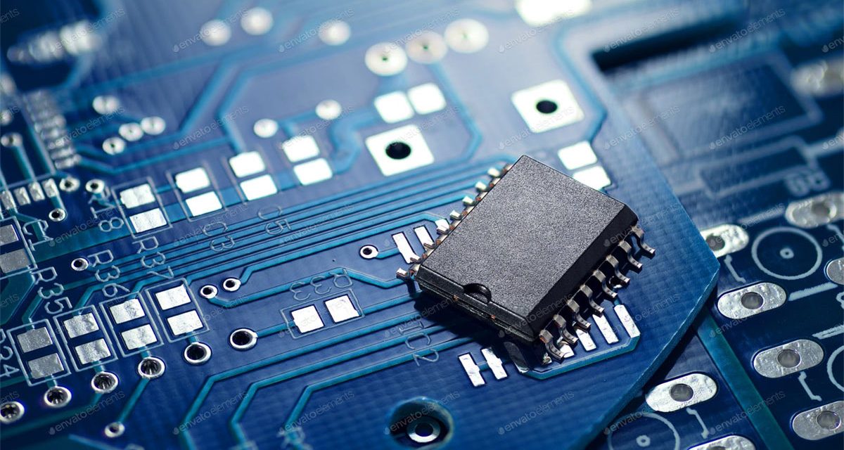
You might not be aware of it, the printed circuit boards are all around us in our day-to-day lives. Printed circuit boards are what power most common household electronics, such as the remote control, radio, or even a doorbell. PCBs are ubiquitous today, so it isn’t surprising that so many businesses are looking to get into this game.
Regardless of their ultimate purpose, if your business produces PCBs then it is vital that you nail the design process. Follow the steps outlined below, and you’ll have no trouble.
Start With Schematics
The first thing that you need to do when designing your own printed circuit board is to lay out the schematics. Before you can think about drawing wires and other components, you need to know what type of circuit you are building. There’s plenty of PCB design software out there that makes putting together the initial schematics nice and simple. Many people find it helpful to first draw their schematic by hand, and then use this as a basis for producing a digital schematic.
One of the most popular and easy to use PCB design software packages out there is Altium. Altium makes the whole process of designing your PCB easy, especially if this is your first time. Don’t bother wrestling with overly-complicated and poorly documented design software.
Optimize Your Design
Once you have your basic schematic down you can then focus on refining your PCB. The optimization process is just as important as the initial design.
In order to optimize your circuit, you will need to divide it into sections and work out what each part is going to do. You should try to keep all the individual functions of your circuit board confined to their own sections. Again, many people find that drawing their design out by hand first makes this part of the process much easier.
One of the most important principles of good PCB design is to ensure that the electrical current is taking the most linear path possible through your circuit board. This means that all the signals flowing through the wires in your board should be taking the most direct route from a to b as possible.
User Interface
Most of the features of a PCB are hidden from the user because they are etched into the interior of the board. However, there are also often going to be a component that the user interacts with directly. A common example of this would be a headphone jack.
When it comes to components that the user interacts with directly, it is very important that they are placed considerately. Some components, such as a power switch, will work best when paired with another component. Most electronic devices today have little LED lights next to the power switch to indicate when the device is turned on.
Designing your own PCBs is challenging at first, but once you know how to do it it becomes a lot more fun. In terms of making your design a reality, there are a number of CAM and 3D printing options available to you. Software packages like Altium can often feed directly into CAD and CAM software, enabling you to move pretty much straight from your schematic to the real thing.


